


U.S. Sub-Nanometer eBeam Market Set for Rapid Growth Through 2036 Fueled by AI Chips, Sub-2nm Process Technologies, and Advanced Semiconductor Metrology
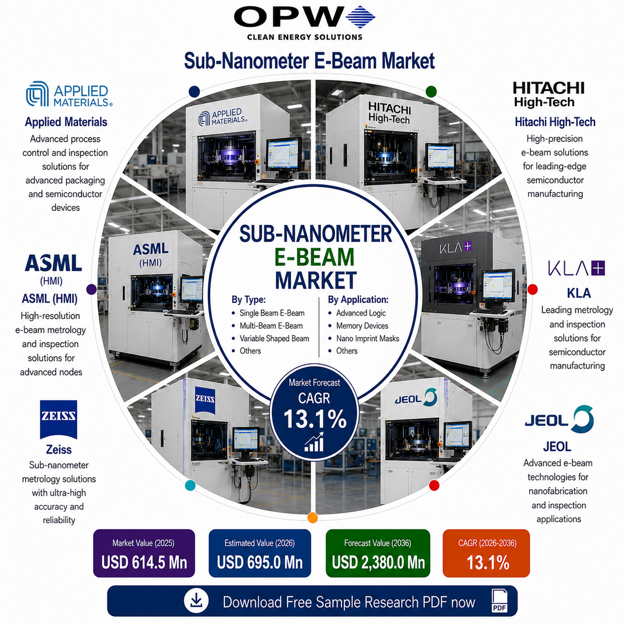
According to a comprehensive market research report published by Fact.MR, The global Sub-Nanometer eBeam Market crossed a valuation of $614.5 million in 2025 and is projected to expand from $695.0 million in 2026 to $2,380.0 million by 2036. This expansion represents a compound annual growth rate (CAGR) of 13.1% over the forecast period, generating an absolute dollar opportunity of $1,685.0 million over the ten-year timeframe.
Get detailed market forecasts, competitive benchmarking, and pricing trends: https://www.factmr.com/connectus/sample?flag=S&rep_id=15674
Market acceleration is primarily driven by leading-edge logic foundries and memory manufacturers requiring sub-nanometer critical dimension control and high-sensitivity defect inspection as advanced transistor architectures scale past sub-2nm nodes.
Key Sub-Nanometer eBeam Market Highlights at a Glance
- Base Year Market Valuation (2025): $614.5 million
- Estimated Market Value (2026): $695.0 million
- Forecast Market Value (2036): $2,380.0 million
- Compound Annual Growth Rate (2026–2036):1%
- Absolute Dollar Opportunity (2026–2036): $1,685.0 million
- Leading System Type Segment: Critical Dimension Scanning Electron Microscope (CD-SEM) systems holding a 32.0% share in 2026
- Leading Resolution Class Segment: Sub-0.5 nanometer (<0.5 nm) resolution capturing a 38.8% market share in 2026
- Leading Beam Architecture Segment: Single-beam columns commanding a 42.4% share in 2026
- Leading Application Segment: Critical dimension metrology leading with a 41.3% share in 2026
- Leading End-User Segment: Pure-play foundries commanding a 29.3% market share in 2026
- Fastest-Growing National Market: United States expanding at a 14.7% CAGR from 2026 to 2036
Why Is the Sub-Nanometer eBeam Market Growing?
Demand for sub-nanometer electron beam (eBeam) metrology and inspection equipment is accelerating rapidly as optical inspection systems reach physical diffraction limits. Three operational imperatives are driving capital equipment acquisition across semiconductor fabs:
- Sensitivity and Throughput Trade-Off at Advanced Nodes: Logic foundries operating sub-2nm processes require sub-nanometer resolution to identify yield-killing edge-placement errors and structural defects that optical inspection cannot detect.
- High-Current Single-Beam Platform Innovations: Toolmakers are integrating multi-signal collection, high current density, and voltage contrast in single-beam architectures to analyze surface, topographic, and deep-trench defects simultaneously.
- Multi-Beam Parallelism Scaling: The deployment of multi-beam arrays with high-speed wafer stages is drastically increasing inspection throughput, allowing fabs to scale high-resolution eBeam coverage across production wafers.
"Sub-nanometer eBeam adoption fundamentally hinges on balancing measurement sensitivity with line throughput at advanced nodes," states Ganesh Pai, Lead Semiconductor Analyst at Fact.MR. "As gate-all-around architectures and high-NA EUV lithography shrink defect margins below one nanometer, fabs are shifting eBeam tools from off-line lab tools to essential process control monitors integrated directly into yield management workflows."
How Does the Sub-Nanometer eBeam Market Break Down Across Segments?
System Type: Why CD-SEM Systems Lead Equipment Spending
CD-SEM systems are projected to represent the leading system type segment, capturing a 32.0% market share in 2026. CD-SEM systems convert high-resolution electron imaging into automated, highly repeatable dimensional measurements essential for maintaining process windows.
- CD-SEM systems market share in 2026: 32.0%
- Primary operational role: Provides calibrated, recipe-driven critical dimension measurement across repeating statistical control workflows
- Alternative system type segments: Targeted eBeam inspection systems, voltage-contrast review tools, and electron-beam lithography modules
Resolution Class: Why <0.5 nm Sub-Nanometer Resolution Leads
The sub-0.5 nanometer (<0.5 nm) resolution class is forecast to hold a commanding 38.8% market share in 2026. Resolution below 0.5 nanometers provides the necessary measurement margin required for tight edge-placement error budgets and line-edge roughness control at leading logic nodes.
- Sub-0.5 nm (<0.5 nm) resolution class market share in 2026: 38.8%
- Process necessity: Resolves sub-nanometer dimensional variation on sub-2nm logic gates and multi-patterned interconnects
- Secondary resolution segment: 0.5–1 nm resolution class serving less aggressive process layers where extreme resolution margins are unnecessary
Beam Architecture: Why Single-Beam Columns Retain Primary Share
Single-beam columns are projected to account for a 42.4% market share in 2026. Single-beam architectures concentrate beam current and detector sensitivity onto a single probe, providing maximum signal-to-noise ratios for complex critical dimension measurements.
- Single-beam column market share in 2026: 42.4%
- Operational advantage: Delivers maximum beam stability and multi-signal detector optimization for targeted defect review
- Emerging architecture segment: Multi-beam arrays leveraging dozens to hundreds of parallel beamlets to expand wafer inspection coverage
Application & End User: Critical Dimension Metrology and Foundry Leadership
Critical dimension metrology leads the application axis with a 41.3% market share in 2026, while pure-play foundries represent the dominant end-user group with a 29.3% market share in 2026. Frequent, recurring sampling in foundries generates a larger installed tool workload than periodic defect review.
- Critical dimension metrology application share in 2026: 41.3%
- Pure-play foundries end-user share in 2026: 29.3%
- Alternative applications and end users: Defect inspection and voltage-contrast review; integrated device manufacturers (IDMs) and advanced memory makers
Sub-Nanometer eBeam Market Dynamics
Market Drivers
The primary driver is the operational demand for sub-nanometer inspection sensitivity where optical inspection fails to deliver sufficient resolution. As features shrink below sub-2nm nodes, measuring critical dimensions, pattern placement, and contact hole integrity requires electron optics.
Market Restraints
The major restraint facing the market is the physical trade-off between inspection resolution and wafer throughput. High-resolution eBeam scans require longer dwelling times per pixel, which can restrict whole-wafer inspection speeds if sampling algorithms are not optimized.
Key Market Trends
A key industry trend is the convergence of high-density single-beam tools with deep-learning defect classification software. Fabs are deploying automated machine learning algorithms to instantly distinguish between cosmetic irregularities and yield-killing electrical defects.
Regional and Country Outlook
Growth in sub-nanometer eBeam equipment spending is concentrated in regions housing leading-edge logic foundries, high-bandwidth memory (HBM) fabs, and semiconductor equipment R&D hubs.
- United States CAGR (2026–2036):7%
- Taiwan CAGR (2026–2036):5%
- South Korea CAGR (2026–2036):0%
- Japan CAGR (2026–2036):5%
- Netherlands CAGR (2026–2036):9%
The United States represents the fastest-growing national market, expanding at a 14.7% CAGR through 2036. Demand in the U.S. is driven by rising onshore leading-edge logic fabrication, domestic semiconductor research programs, and high-performance computing hardware development.
Taiwan is forecast to expand at a 14.5% CAGR, supported by massive commercial foundry expansions, advanced wafer-level packaging centers, and sub-2nm manufacturing roadmaps.
South Korea is projected to register a 14.0% CAGR, propelled by aggressive high-bandwidth memory (HBM) and next-generation DRAM scale-up requiring tight contact-hole metrology.
Japan is expected to grow at a 13.5% CAGR, anchored by robust optical and electron metrology research facilities, specialty wafer processing, and material inspection hubs.
The Netherlands is forecast to record a 12.9% CAGR through 2036, supported by world-leading semiconductor lithography and electron-beam metrology equipment R&D ecosystems.
Competitive Landscape
The competitive environment in the sub-nanometer eBeam market features established semiconductor metrology giants and high-precision electron-beam tool pioneers.
- Applied Materials: Global supplier of advanced eBeam metrology platforms and high-throughput voltage-contrast inspection systems.
- KLA Corporation: Market leader in automated inspection offering single-beam eBeam platforms with multi-signal detection capabilities.
- ASML (HMI): Pioneer in multi-beam electron inspection platforms designed for high-speed wafer surface scanning.
- Hitachi High-Tech: Key manufacturer of high-precision CD-SEM systems utilized worldwide for inline critical dimension measurement.
- ZEISS: Provider of high-resolution electron optics, photomask inspection systems, and sub-nanometer analytical review tools.
Tool providers are competing on scan velocity, beam stability, multi-signal detector integration, and automated machine-learning software capable of speeding up yield analysis.
Read the Comprehensive Industry Report: https://www.factmr.com/report/sub-nanometer-ebeam-market
Frequently Asked Questions (FAQ)
What is the projected market size of the Sub-Nanometer eBeam Market by 2036?
The global Sub-Nanometer eBeam Market is projected to reach a valuation of $2,380.0 million by 2036.
What is the expected growth rate (CAGR) for the Sub-Nanometer eBeam Market?
The Sub-Nanometer eBeam Market is expected to expand at a compound annual growth rate (CAGR) of 13.1% between 2026 and 2036.
Which system type segment leads the market share?
CD-SEM systems represent the leading system type segment, holding a projected 32.0% market share in 2026.
Which resolution class accounts for the largest market share?
The sub-0.5 nanometer (<0.5 nm) resolution class leads the market, holding a 38.8% share in 2026.
Which application holds the highest share in the Sub-Nanometer eBeam Market?
Critical dimension metrology is the leading application segment, capturing a 41.3% market share in 2026.
Which country is forecast to be the fastest-growing market?
The United States is forecast to be the fastest-growing national market, expanding at a 14.7% CAGR from 2026 to 2036.
Who are the key players operating in the Sub-Nanometer eBeam Market?
Key companies operating in the market include Applied Materials, KLA Corporation, ASML (HMI), Hitachi High-Tech, and ZEISS.
To View Related Report:
Backside Via Inspection Market: https://www.factmr.com/report/backside-via-inspection-market
GAA Epitaxy Systems Market: https://www.factmr.com/report/gaa-epitaxy-systems-market
Backside Power Metrology Market: https://www.factmr.com/report/backside-power-metrology-market
High-Aspect Cryoetch Market: https://www.factmr.com/report/high-aspect-cryoetch-market
View More Report:
Post-Quantum Migration Services Market: https://www.openpr.com/news/4588759/u-s-post-quantum-migration-services-market-size-to-hit-usd-55-0
Carbon Removal MRV Services Market: https://www.openpr.com/news/4588797/u-s-carbon-removal-mrv-services-market-size-to-hit-usd-15-0

 English
 Arabic
 French
 Spanish
 Portuguese
 Deutsch
 Turkish
 Dutch
Dutch
 Italiano
 Romaian
 Portuguese (Brazil)
 Greek
Greek
