


Semiconductor Wafer Mounting Systems Market
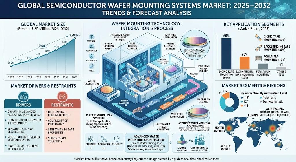
The global Semiconductor Wafer Mounting Systems Market was valued at USD 114 million in 2025 and is projected to reach USD 185 million by 2034, growing at a CAGR of 7.3% during the forecast period. The market is gaining steady momentum as semiconductor manufacturing continues to expand globally, particularly in advanced packaging and high-performance computing applications. Wafer mounting systems play a critical role in the back-end semiconductor process by securely attaching thinned wafers onto dicing tape or film, ensuring protection during dicing and handling while minimizing contamination and damage.
Growing Demand from Advanced Packaging Technologies
The rapid evolution of advanced semiconductor packaging technologies, including 2.5D/3D integration and fan-out wafer-level packaging (FOWLP), is a key driver for the Semiconductor Wafer Mounting Systems Market. These technologies require high precision in wafer handling and temporary bonding processes to maintain structural integrity and performance. As chipmakers continue to develop smaller, more powerful devices, demand for sophisticated wafer mounting systems capable of controlling stress, alignment, and warpage is increasing significantly.
Expansion of Semiconductor Industry Fuels Market Growth
The overall growth of the global semiconductor industry is directly supporting the demand for wafer mounting systems. Increasing investments in fabrication plants and packaging facilities, particularly in Asia-Pacific and the Americas, are creating strong demand for backend equipment. Growth in memory and logic semiconductor segments is further accelerating the need for high-throughput and automated mounting solutions to ensure production efficiency and yield optimization.
Rising Adoption of Compound Semiconductors
The increasing use of compound semiconductors such as gallium nitride (GaN) and silicon carbide (SiC) is further boosting market demand. These materials are widely used in power electronics, electric vehicles, and RF applications due to their superior performance characteristics. However, their fragile and thin nature requires specialized wafer mounting systems designed to handle unique material properties, driving innovation and investment in next-generation equipment.
Automation and Smart Manufacturing Trends
Automation is becoming a central trend in the Semiconductor Wafer Mounting Systems Market, with manufacturers focusing on fully automated solutions to improve throughput and reduce contamination in cleanroom environments. Integration with smart manufacturing technologies, including sensors, in-line metrology, and AI-driven process control, is enabling real-time monitoring and predictive maintenance. These advancements are helping semiconductor manufacturers achieve higher efficiency, improved yields, and reduced operational costs.
Challenges in Process Complexity and Cost Sensitivity
Despite positive growth prospects, the market faces challenges related to technical complexity and high capital investment. Integrating wafer mounting systems into advanced semiconductor production lines requires precise control of multiple parameters, including adhesive properties, temperature, and debonding processes. Additionally, high equipment costs can be a barrier for smaller manufacturers, while price sensitivity in mature semiconductor segments limits the adoption of premium systems.
Opportunities in AI, Chiplet Architectures, and Emerging Technologies
The growing adoption of chiplet-based architectures and AI accelerators presents significant opportunities for the market. These technologies rely heavily on precise wafer-level processing, including thinning and bonding, creating demand for advanced mounting systems capable of handling ultra-thin wafers with high accuracy. Furthermore, increasing demand for high-performance computing and data centers is expected to drive further investment in semiconductor packaging technologies.
Asia-Pacific Leads Market Expansion
Asia-Pacific dominates the Semiconductor Wafer Mounting Systems Market, driven by strong semiconductor manufacturing ecosystems in countries such as Japan, China, South Korea, and Taiwan. The region continues to witness significant investments in fabrication and packaging facilities, making it a key growth hub. North America and Europe also contribute to market growth through technological innovation and increasing focus on supply chain resilience.
Competitive Landscape
The market is highly consolidated, with Japanese companies leading the global landscape through advanced engineering and strong supply chain integration. Key players include Nitto Denko, LINTEC Corporation, DISCO Corporation, and Takatori Corporation. These companies are focusing on product innovation, automation, and material advancements to strengthen their market position and meet evolving industry demands.
Market Segmentation Highlights
By Type
Fully Automatic Systems
Semi-Automatic Systems
Manual Systems
By Application
Memory Devices
Logic Devices
Power Devices
RF Devices
By End User
Semiconductor Foundries
Outsourced Semiconductor Assembly and Test (OSAT) Providers
Integrated Device Manufacturers
By Wafer Size
6-inch
8-inch
12-inch
Get Full Report Here:
Narrowband Multispectral Filter Market, Trends, Business Strategies 2026-2034
About Semiconductorinsight
Semiconductor Insight is a leading provider of market intelligence and strategic consulting for the global semiconductor and high‑technology industries. Our in‑depth reports and analysis offer actionable insights to help businesses navigate complex market dynamics, identify growth opportunities, and make informed decisions. We are committed to delivering high‑quality, data‑driven research to our clients worldwide.
🌐 Website: https://semiconductorinsight.com/
📞 International: +91 8087 99 2013
🔗 LinkedIn: Follow Us

 English
 Arabic
 French
 Spanish
 Deutsch
 Turkish
 Dutch
Dutch
 Italiano
 Russian
 Romaian
 Portuguese (Brazil)
 Greek
Greek
