


Semiconductor Inspection Equipment Market,
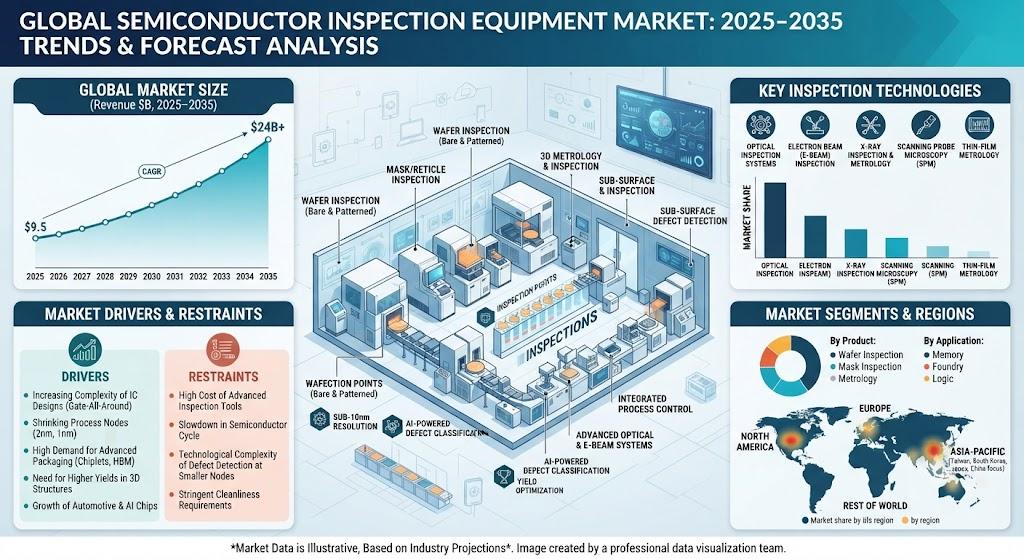
Semiconductor Inspection Equipment Market, valued at USD 8,879 million in 2024, is poised for steady growth, projected to increase from USD 9,320 million in 2025 to USD 12,380 million by 2032. This represents a compound annual growth rate (CAGR) of 5.0% during the forecast period, according to a comprehensive new analysis by Semiconductor Insight. The report underscores the indispensable role of inspection and metrology systems in maintaining the integrity and yield of semiconductor manufacturing, a sector where nanometer-scale defects can lead to catastrophic financial losses.
Semiconductor inspection equipment, crucial for identifying defects and measuring critical dimensions during chip fabrication, has become a cornerstone of modern electronics production. As transistor densities increase and geometries shrink below 5 nanometers, the need for sophisticated inspection technologies capable of detecting sub-nanometer imperfections has intensified, making these systems vital for maintaining high yields in advanced manufacturing processes. The equipment's ability to provide real-time process control and rapid feedback loops allows manufacturers to quickly identify and correct process deviations, significantly reducing scrap and improving overall operational efficiency.
Strategic Imperative: The Critical Role of Inspection in Semiconductor Manufacturing
The relentless advancement of semiconductor technology serves as the primary catalyst for inspection equipment demand. As the industry transitions to more complex 3D architectures like gate-all-around transistors and advanced packaging schemes such as chiplets, the inspection challenges multiply exponentially. This technological evolution directly correlates with increased inspection intensity throughout the fabrication process. With semiconductor manufacturing involving up to 600 process steps for advanced nodes, the probability of defects increases substantially, making comprehensive inspection protocols not just beneficial but absolutely essential for economic viability.
"The transition to advanced nodes below 7nm has fundamentally altered the inspection landscape," the report emphasizes. "Where optical inspection once sufficed, manufacturers now require hybrid systems combining multiple technologies to detect defects that were previously undetectable. The Asia-Pacific region, housing over 75% of global semiconductor manufacturing capacity, represents the most significant market for inspection equipment, with leading foundries and memory manufacturers continuously upgrading their inspection capabilities to maintain competitive yields." The push toward angstrom-level manufacturing at 2nm and beyond is creating unprecedented demand for inspection systems with atomic-scale resolution.
Read Full Report: https://semiconductorinsight.com/report/semiconductor-inspection-equipment-market/
Market Segmentation: Defect Inspection and Wafer Applications Lead Growth
The report delivers a thorough segmentation analysis, providing valuable insights into market structure and high-growth areas:
Segment Analysis:
By Type
-
Defect Inspection Equipment
-
Metrology Equipment
By Application
-
Semiconductor Wafer Inspection
-
Semiconductor Mask/Film Inspection
-
Others
By End User
-
Integrated Device Manufacturers (IDMs)
-
Foundries
-
Memory Manufacturers
By Technology
-
Optical Inspection
-
E-beam Inspection
-
Hybrid/Multi-Beam Inspection
By Component
-
Hardware
-
Software
-
Services
Download Sample Report: https://semiconductorinsight.com/download-sample-report/?product_id=127115
Competitive Landscape: Technology Leaders and Strategic Focus
The analysis profiles key market participants who are shaping the industry's trajectory, including:
-
KLA Corporation
-
ASML Holding N.V.
-
Lasertec Corporation
-
Carl Zeiss AG
-
SCREEN Semiconductor Solutions Co., Ltd.
-
Camtek Ltd.
-
Veeco Instruments Inc.
-
Toray Engineering Co., Ltd.
-
Muetec GmbH
-
Unity Semiconductor SAS
-
Microtronic
-
RSIC Scientific Instrument
Market leaders are aggressively pursuing technological differentiation through artificial intelligence and machine learning integration, which enhances defect detection accuracy while reducing false positives. Companies are also expanding their service and support infrastructure globally to provide faster response times and minimize equipment downtime for their customers. Furthermore, strategic partnerships with semiconductor manufacturers for co-development of application-specific inspection solutions represent a key competitive strategy, particularly for addressing the unique challenges of next-generation nodes.
Emerging Opportunities in Advanced Packaging and AI-Driven Inspection
Beyond traditional front-end manufacturing, several emerging trends are creating new growth vectors. The rapid adoption of advanced packaging technologies, particularly for heterogeneous integration and 3D chip stacking, requires specialized inspection solutions capable of verifying interconnects and detecting defects in complex 3D structures. Similarly, the integration of artificial intelligence and machine learning algorithms represents a paradigm shift, enabling predictive maintenance and significantly enhanced defect classification accuracy. The industry is also witnessing increased demand for inspection solutions tailored to compound semiconductors and novel materials like silicon carbide and gallium nitride, which are essential for power electronics and RF applications.
Report Scope and Strategic Implications
The market research report provides an exhaustive analysis of the global Semiconductor Inspection Equipment market from 2025 to 2032. It encompasses detailed market segmentation, precise size forecasts, competitive intelligence, emerging technology assessment, and comprehensive evaluation of key market dynamics. The analysis identifies critical success factors and potential disruptors that could reshape the competitive landscape.
For strategic insights into market drivers, technological barriers, emerging opportunities, and competitive positioning strategies, the complete report offers essential intelligence.
Download FREE Sample Report: Semiconductor Inspection Equipment Market - View in Detailed Research Report
Get Full Report Here: Semiconductor Inspection Equipment Market, Global Business Strategies 2025-2032 - View in Detailed Research Report
About Semiconductor Insight
Semiconductor Insight is a leading provider of market intelligence and strategic consulting for the global semiconductor and high-technology industries. Our in-depth reports and analysis offer actionable insights to help businesses navigate complex market dynamics, identify growth opportunities, and make informed decisions. We are committed to delivering high-quality, data-driven research to our clients worldwide.
🌐 Website: https://semiconductorinsight.com/
📞 International: +91 8087 99 2013
🔗 LinkedIn: Follow Us

 English
 Arabic
 French
 Spanish
 Portuguese
 Deutsch
 Dutch
Dutch
 Italiano
 Russian
 Romaian
 Portuguese (Brazil)
 Greek
Greek
