


3D IC and 2.5D IC Packaging Market Benefits from Rapid Chiplet Technology Adoption
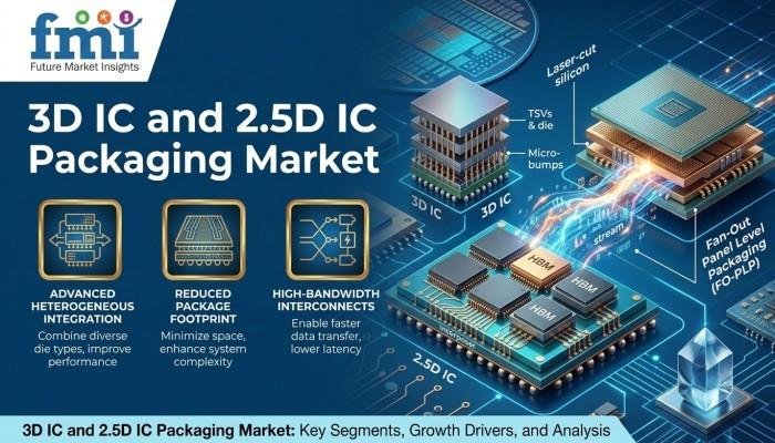
The global 3D IC and 2.5D IC packaging market is entering a high-growth phase as semiconductor manufacturers and system designers respond to rising demand for higher bandwidth, lower latency, and greater integration density. According to the latest market analysis by Future Market Insights (FMI), the market was valued at USD 58.30 billion in 2025 and is expected to increase to USD 63.55 billion in 2026. Over the forecast period from 2026 to 2036, the market is projected to surge to USD 150.44 billion, expanding at a CAGR of 9.00%.
The market is set to add approximately USD 86.89 billion in absolute terms between 2026 and 2036, driven primarily by the rapid adoption of AI accelerators, high-bandwidth memory (HBM), and advanced chiplet-based architectures. As data center GPU and TPU deployments accelerate, conventional 2D packaging is increasingly unable to meet the interconnect density and memory bandwidth requirements of next-generation semiconductor devices.
3D IC and 2.5D IC packaging technologies, which rely on through-silicon vias (TSVs), silicon interposers, and wafer-level chip-scale packaging, are becoming essential for vertically and laterally integrating multiple die into a single package. These technologies are enabling compact, high-performance designs across logic, memory, imaging, sensor, LED, telecom, automotive, and medical applications.
Get detailed market forecasts, competitive benchmarking, and pricing trends:
https://www.futuremarketinsights.com/reports/sample/rep-gb-25260
Market Overview and Strategic Growth Outlook
The 3D IC and 2.5D IC packaging market is being transformed by the semiconductor industry’s push toward heterogeneous integration, miniaturization, and thermal efficiency. Demand from AI infrastructure is creating unprecedented pressure on packaging capacity, particularly for advanced platforms such as TSMC CoWoS and Intel EMIB, which are directly aligned with the packaging requirements of leading chip designers.
HBM manufacturers including SK Hynix, Samsung, and Micron are also fueling adoption of TSV-based 3D stacking, as AI GPUs increasingly require multiple HBM stacks per package. In parallel, the automotive sector is emerging as a new growth frontier, with sensor fusion modules integrating LiDAR ASICs, radar processors, and vision processors into advanced 2.5D packages.
Key Market Projections and Strategic Insights
- Global Market Value (2026): USD 63.55 Billion
- Forecast Market Value (2036): USD 150.44 Billion
- Forecast CAGR (2026–2036): 9.00%
- Leading Technology Segment: 3D TSV
- Technology Segment Share: 50.6%
- Leading Application Segment: Logic
- Application Share: 45.9%
- Leading End-Use Segment: Consumer Electronics
- End-Use Share: 38.4%
- Fastest Growing Market: China
- China CAGR: 12.20%
- India CAGR: 11.30%
- Key Growth Regions: Asia Pacific, North America, Europe
Competitive Landscape and Market Share Analysis
The competitive environment remains highly dynamic, with global semiconductor companies and OSAT providers investing heavily in packaging innovation, capacity expansion, and ecosystem partnerships.
Key companies operating in the market include:
- TSMC (Taiwan Semiconductor Manufacturing Company)
- Advanced Semiconductor Engineering (ASE)
- Amkor Technology
- Broadcom
- ChipMOS Technologies Inc.
- Intel Corporation
- Jiangsu Changjiang Electronics Technology (JCET)
- Mitsubishi Electric Corporation
- Powertech Technology Inc. (PTI)
- Samsung Electronics
- Siliconware Precision Industries (SPIL)
- Texas Instruments
- Toshiba Corporation
- United Microelectronics Corporation (UMC)
- Xilinx Inc.
Manufacturers are actively investing in:
- TSV fabrication and vertical interconnect technologies
- Silicon interposer platforms for high-bandwidth communication
- Advanced wafer-level packaging solutions
- Thermal management and power efficiency improvements
- HBM-compatible 3D stacking systems
- Heterogeneous integration for AI and chiplet architectures
Production Analysis and Manufacturing Landscape
Production of 3D IC and 2.5D IC packaging solutions is concentrated in regions with advanced semiconductor ecosystems, strong foundry capabilities, and robust OSAT infrastructure.
Asia Pacific remains the leading manufacturing hub due to:
- Large-scale semiconductor production capacity
- Strong advanced packaging investments
- Cost-efficient manufacturing ecosystems
- Rising domestic demand from consumer electronics and AI infrastructure
- Government support for semiconductor self-sufficiency
North American producers are focusing on advanced node integration, AI infrastructure, defense applications, and data center demand, while European manufacturers are emphasizing automotive electronics, industrial applications, and high-reliability packaging solutions.
Consumption Economy Analysis
Demand trends are closely tied to the expansion of AI computing, mobile electronics, automotive semiconductor adoption, and hyperscale data center investments.
Major consumption sectors include:
- Consumer electronics
- Telecommunication infrastructure
- Automotive electronics
- Military and aerospace systems
- Medical devices
- Smart technologies
- Data center and AI accelerator platforms
Consumer electronics remains the largest end-use segment, accounting for 38.4% of total demand in 2026, supported by smartphones, tablets, wearables, and compact high-performance devices.
Country Opportunity Assessment
China
China is projected to remain the fastest-growing market with a CAGR of 12.20%, supported by government-backed semiconductor policies, expanding foundry capabilities, and scale-driven adoption of advanced packaging in AI, 5G, and consumer electronics.
India
India is expected to grow at 11.30% CAGR through 2036, driven by domestic electronics manufacturing, telecom infrastructure, cloud expansion, and “Make in India” semiconductor initiatives.
Germany
Germany is forecast to expand at 10.40% CAGR, supported by automotive electronics, industrial automation, and precision-focused semiconductor adoption.
United States
The U.S. market is projected to grow at 7.70% CAGR, supported by AI computing, defense electronics, hyperscale cloud infrastructure, and advanced packaging R&D.
France and the UK
France and the UK are witnessing steady growth through research-led semiconductor programs, design innovation, automotive applications, and strategic partnerships with advanced packaging ecosystems.
Technology and Innovation Outlook
The industry is evolving rapidly through:
- 3D TSV packaging
- 3D wafer-level chip-scale packaging
- 2.5D silicon interposer integration
- High-density heterogeneous chiplet design
- Advanced thermal dissipation solutions
- HBM-compatible packaging architectures
Market Drivers Accelerating Industry Expansion
Primary growth drivers include:
- Rising AI accelerator demand
- Expanding HBM adoption
- Growth in data center GPU and TPU deployments
- Increasing use of chiplet-based architectures
- Greater demand for miniaturization and performance optimization
- Automotive sensor fusion and ADAS integration
- Continued investment in advanced semiconductor packaging capacity
Related Reports:
https://www.openpr.com/news/4572355/corrugated-automotive-packaging-market-size-to-reach-usd-34-5
Business Impact
FMI helps organizations transform market complexity into strategic clarity, enabling leadership teams to identify growth opportunities faster, optimize resource allocation, strengthen competitive positioning, and make high-stakes business decisions with confidence.
To explore how FMI Custom Research can support your strategic priorities, please connect with our team at - sales@futuremarketinsights.com
About Future Market Insights (FMI)
Future Market Insights, Inc. (FMI) is an ESOMAR-certified, ISO 9001:2015 market research and consulting organization, trusted by Fortune 500 clients and global enterprises. With operations in the U.S., UK, India, and Dubai, FMI provides data-backed insights and strategic intelligence across 30+ industries and 1200 markets worldwide.

 English
 Arabic
 French
 Spanish
 Portuguese
 Deutsch
 Turkish
 Dutch
Dutch
 Italiano
 Romaian
 Portuguese (Brazil)
 Greek
Greek
