Chemical Mechanical Planarization Industry Projected to Reach US$ 11.91 Billion by 2033
The global Chemical Mechanical Planarization Industry is experiencing significant growth, driven by the increasing complexity of semiconductor devices, rising demand for advanced integrated circuits, and continuous innovation in electronics manufacturing processes. Chemical mechanical planarization (CMP) plays a vital role in achieving ultra-flat wafer surfaces, enabling the production of high-performance chips used in consumer electronics, automotive systems, telecommunications, and data centers.
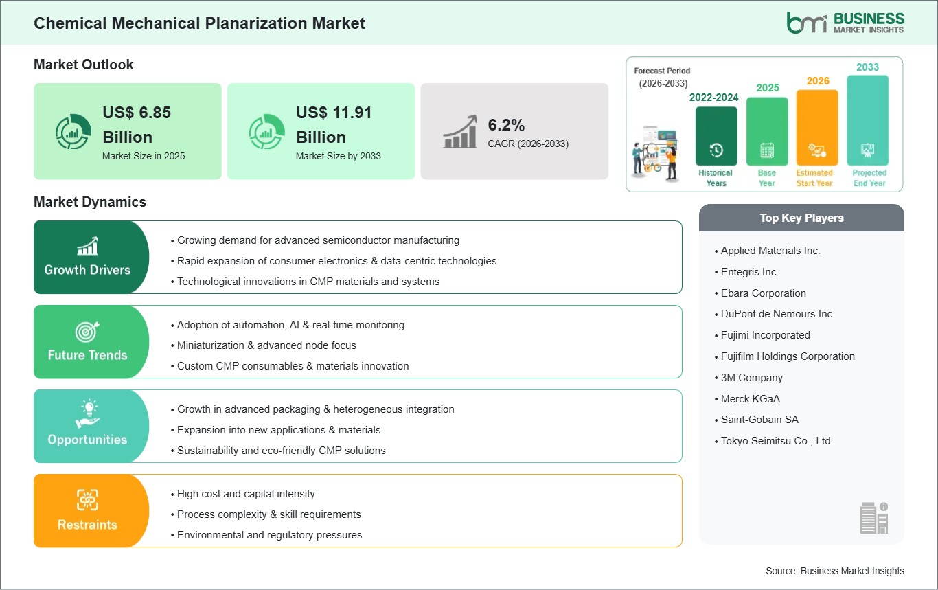
According to Business Market Insights, the global Chemical Mechanical Planarization Market is projected to grow from US$ 6.85 billion in 2025 to US$ 11.91 billion by 2033. The market is expected to register a CAGR of 7.16% during the forecast period from 2026 to 2033.
As modern electronics rely increasingly on complex multilayer chips, CMP equipment and consumables serve as a critical operational backbone. By providing precision systems essential for increasingly complex device architectures, the CMP process minimizes manufacturing yield losses. Capital investment within the industry is heavily focusing on automated systems, real-time process monitoring, and the optimization of slurries and polishing pads to ensure ultra-flat surfaces in integrated circuits and memory chips.
What Is Chemical Mechanical Planarization?
Chemical Mechanical Planarization (CMP) is a critical manufacturing process used in the semiconductor industry to smooth surfaces with the combination of chemical and mechanical forces. The process utilizes specialized CMP equipment and tailored consumables, such as abrasive chemical slurries and polishing pads, to remove irregular topography on the surface of a silicon wafer. This ensures wafer-level flatness and defect-free surfaces, which are absolutely essential for high-performance computing, consumer electronics, and modern 5G devices.
During the fabrication of integrated circuits, multiple layers of conducting and insulating materials are deposited onto the wafer. Without precise planarization, subsequent layers cannot be accurately patterned using photolithography. By deploying advanced CMP techniques, semiconductor manufacturers can achieve the ultra-flat, high-precision surfaces required to build complex, miniaturized, and high-performance microchips with minimal yield loss.
Download Sample Report: https://www.businessmarketinsights.com/sample/BMIPUB00033286
Market Drivers
A primary driver accelerating the global Chemical Mechanical Planarization Industry is the Rising Demand for Miniaturized and High-Performance Semiconductors. The market is primarily driven by the increasing demand for smaller, more powerful semiconductor devices across the consumer electronics, automotive, telecommunications, and computing industries. As device form factors shrink, achieving flawless, ultra-flat surfaces becomes a non-negotiable requirement, driving intense demand for advanced CMP solutions.
The Continual Advancements in 5G, IoT, and High-Performance Computing serves as another core driver. The deployment of complex multilayer chips required to power modern 5G networks, artificial intelligence hardware, and the expanding Internet of Things requires sophisticated planarization techniques. These high-end electronics depend on CMP to guarantee structural integrity and peak performance at microscopic scales.
Additionally, Escalating Global Semiconductor Production Investments acts as a major market catalyst. Countries worldwide are investing heavily in new semiconductor fabrication facilities to meet growing domestic and global demand. The establishment of advanced IC production lines and extensive investments in wafer fabrication necessitate the massive procurement of high-precision CMP equipment and ongoing supplies of polishing consumables.
Market Segmentation
By Equipment
- CMP Equipment (Dominated the market in 2025 due to its critical role in achieving high-precision planarization for advanced semiconductor devices; reinforced by advancements in automated systems and real-time process monitoring)
- CMP Consumables (Experiencing continuous growth as manufacturers require a steady supply of specialized slurries and polishing pads to optimize processes and manufacturing yields)
By Application
- Integrated Circuits (Held the largest share of the market in 2025, driven by the fact that modern electronics rely on complex multilayer chips necessitating perfect wafer-level flatness)
- Compound Semiconductors (Represents a major segment due to extensive use in high-end electronics, telecommunications equipment, and optoelectronics)
- MEMS and NEMS (Sustained by the growing integration of micro-electromechanical and nano-electromechanical systems in consumer and automotive sensors)
- Other Application (Encompasses emerging semiconductor architectures and specialized memory chip planarization needs)
Regional Insights
- Asia Pacific dominates the global Chemical Mechanical Planarization market and leads revenue generation. This is driven by the dense concentration of semiconductor manufacturing hubs in China, Japan, South Korea, Taiwan, and India. The region benefits massively from rapid industrialization, extensive investments in wafer fabrication, and advanced consumer electronics manufacturing.
- North America captures a substantial portion of global revenues, anchored by the United States and Canada. Strong investments in semiconductor research and the presence of leading high-performance computing and automotive technology developers support consistent demand for CMP processes.
- Europe displays robust demand supported by nations such as Germany, the UK, and France. The region's automotive manufacturing sector and strategic moves to increase domestic integrated circuit production drive the adoption of sophisticated planarization equipment.
- Rest of the World (including South & Central America and the Middle East & Africa) accounts for progressive market growth as localized tech infrastructure projects and telecommunications upgrades drive peripheral demand for semiconductor devices.
Top Players in the Industry
The competitive ecosystem of the chemical mechanical planarization sector is characterized by the presence of specialized equipment manufacturers and advanced materials providers focusing on high manufacturing yield and precision.
- Applied Materials Inc.
- Entegris Inc.
- Ebara Corporation
- DuPont de Nemours Inc.
- Fujimi Incorporated
- Fujifilm Holdings Corporation
- 3M Company
- Merck KGaA
- Saint-Gobain SA
- Tokyo Seimitsu Co., Ltd.
Strategic Industry Challenges
Despite strong global demand, the CMP market faces challenges related to the increasing complexity of device architectures. As semiconductor designs transition to multi-layered, 3D structures, the planarization process demands unprecedented levels of precision. Manufacturers must continually invest heavily in research and development to create new slurries and polishing pads capable of handling diverse new materials without causing surface defects, scratching, or yield losses, adding significant operational costs to fabrication facilities.
Future Market Outlook
The forward trajectory for the Chemical Mechanical Planarization Market remains exceptionally robust. The persistent global push for miniaturization, combined with the expanding footprint of the automotive and telecommunications sectors, ensures that advanced planarization techniques will remain an absolute baseline requirement. As manufacturers continue to optimize their processes, the integration of real-time monitoring and automated CMP equipment will dictate the next wave of high-performance semiconductor fabrication.
Frequently Asked Questions (FAQs)
What is the projected size of the global Chemical Mechanical Planarization Market by 2033?
The market is projected to reach an estimated valuation of US$ 11.91 Billion by 2033, growing from an established base of US$ 6.85 Billion in 2025.
Which application segment held the largest market share?
The Integrated Circuits segment held the largest share of the market in 2025, as modern high-performance computing and 5G devices rely heavily on complex, defect-free multilayer chips.
Which region leads the global CMP market?
Asia Pacific dominates the global market, driven by the heavy concentration of leading semiconductor manufacturing hubs and extensive wafer fabrication investments in countries like China, South Korea, Japan, and Taiwan.
Browse More Reports:
Cable Testing Certification Market
Distributed Fiber Optic Sensor Market
About Us
Business Market Insights is a market research platform that provides subscription service for industry and company reports. Our research team has extensive professional expertise in domains such as Aerospace & Defense; Automotive & Transportation; Electronics & Semiconductor; Energy & Power; Healthcare; Manufacturing & Construction; Food & Beverages; Chemicals & Materials; and Technology, Media, & Telecommunications.
Contact Us
If you have any questions about this report or would like further information, please contact us:
Contact person: Ankit Mathur
Email: sales@businessmarketinsights.com
Phone: +16467917070