


Semiconductor Materials for CMP Market
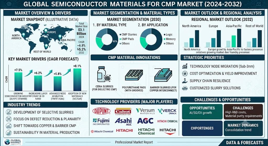
Global Semiconductor Materials for CMP Market was valued at approximately USD 3.38 billion in 2024 and is projected to reach USD 5.46 billion by 2032, growing at a CAGR of 7.3% during the forecast period.
Semiconductor materials for Chemical Mechanical Planarization (CMP) are critical consumables used during wafer fabrication to achieve ultra-flat and defect-free surfaces. The market includes CMP slurries, polishing pads, pad conditioners, slurry filters, PVA brushes, and retaining rings. These materials play a crucial role in advanced semiconductor manufacturing by enabling precise planarization, improving lithography accuracy, and enhancing overall chip performance.
Advanced Semiconductor Nodes Drive Demand for High-Precision CMP Materials
The semiconductor industry's transition toward increasingly advanced process nodes continues to drive demand for sophisticated CMP materials.
Key growth drivers include:
-
Expansion of sub-7nm semiconductor production
-
Growing adoption of 3nm and 2nm technologies
-
Increasing wafer complexity
-
Rising AI and high-performance computing demand
-
Greater focus on yield optimization
-
Growth of advanced memory technologies
As device geometries continue shrinking, achieving atomic-level surface smoothness has become essential, significantly increasing CMP material consumption across semiconductor fabs.
Semiconductor Fab Expansion Creates Strong Market Opportunities
Massive investments in global semiconductor manufacturing capacity are boosting demand for CMP consumables.
Major industry developments include:
-
New wafer fabrication plants across Asia-Pacific
-
Semiconductor reshoring initiatives in North America
-
European semiconductor sovereignty programs
-
Expansion of foundry manufacturing capacity
-
Rising memory chip production investments
-
Government-backed semiconductor development programs
Each advanced semiconductor fabrication facility consumes significant volumes of CMP materials annually, making fab expansion a major growth catalyst for the industry.
Advanced Packaging Technologies Accelerate Specialized CMP Material Demand
Emerging semiconductor packaging technologies are creating new opportunities for CMP material manufacturers.
Key technology trends include:
-
3D IC packaging
-
Hybrid bonding technologies
-
Through-Silicon Via (TSV) integration
-
Fan-Out Wafer Level Packaging (FOWLP)
-
Chiplet architectures
-
Heterogeneous integration platforms
These advanced packaging approaches require highly specialized CMP slurries and polishing materials capable of handling multiple substrate materials with exceptional precision.
Emerging Memory Technologies Drive CMP Innovation
The growing adoption of advanced memory architectures is increasing demand for next-generation CMP solutions.
Important application areas include:
-
3D NAND flash memory
-
MRAM technologies
-
FeRAM devices
-
High-bandwidth memory (HBM)
-
DRAM scaling
-
AI memory architectures
As memory manufacturers continue increasing layer counts and device complexity, CMP materials are becoming increasingly critical for maintaining performance and production yields.
Market Segmentation: CMP Slurry Dominates Global Demand
The Semiconductor Materials for CMP Market is segmented by product type, application, end-user, and technology node.
By Type
-
CMP Slurry
-
CMP Pads
-
CMP Pad Conditioners
-
CMP POU Slurry Filters
-
CMP PVA Brushes
-
CMP Retaining Rings
The CMP Slurry segment dominates the market due to:
-
Critical role in material removal
-
High consumption volume
-
Advanced formulation requirements
-
Continuous innovation cycles
-
Broad application across fabrication processes
CMP slurries represent the largest revenue-generating segment within the CMP materials ecosystem.
By Application
-
300mm Wafers
-
200mm Wafers
-
Others
The 300mm Wafer segment accounts for the largest market share because:
-
Dominance in advanced semiconductor production
-
Higher manufacturing efficiency
-
Large-scale foundry adoption
-
Greater output requirements
The industry's transition toward larger wafer sizes continues to strengthen demand for CMP consumables optimized for 300mm processing.
By End User
-
Foundries
-
IDMs (Integrated Device Manufacturers)
-
OSAT Companies
-
Research Institutes
The Foundry segment remains the leading end-user category due to:
-
Large-scale semiconductor manufacturing
-
Advanced process node deployment
-
High wafer production volumes
-
Growing fab capacity investments
Leading foundries consume substantial quantities of CMP materials across multiple manufacturing stages.
By Technology Node
-
Below 10nm
-
10nm–20nm
-
20nm–45nm
-
Above 45nm
The Below 10nm segment is experiencing the fastest growth as advanced node manufacturing requires extremely precise planarization and contamination control.
Emerging CMP Technologies Improve Efficiency and Sustainability
The CMP industry continues to innovate through the development of advanced polishing technologies and environmentally sustainable solutions.
Key technological advancements include:
-
Ultra-fine nanoparticle slurry formulations
-
Low-defect polishing technologies
-
Advanced polyurethane pad materials
-
Closed-loop slurry recycling systems
-
Green chemistry CMP solutions
-
Enhanced pad conditioning technologies
These innovations help semiconductor manufacturers achieve:
-
Improved wafer yields
-
Reduced defect density
-
Lower operating costs
-
Enhanced process consistency
-
Better environmental performance
Competitive Landscape: Industry Leaders Focus on Innovation and Market Consolidation
The Semiconductor Materials for CMP market remains highly consolidated, with leading companies focusing on technology development, acquisitions, and strategic partnerships.
Key companies include:
-
Fujifilm Holdings
-
Resonac Corporation
-
Fujimi Incorporated
-
DuPont
-
Merck KGaA
-
AGC Inc.
-
KC Tech
-
JSR Corporation
-
Entegris
-
3M
-
Pall Corporation
-
Kinik Company
-
Fujibo Holdings
-
Hubei Dinglong
Competitive strategies focus on:
-
Advanced slurry development
-
Next-generation pad technologies
-
Sustainability initiatives
-
Strategic acquisitions
-
Capacity expansion
-
Semiconductor foundry partnerships
Recent consolidation activities continue reshaping the competitive landscape as companies seek integrated CMP solution portfolios.
Challenges: High Development Costs and Supply Chain Complexity Remain Key Barriers
Despite strong market growth, several challenges continue to impact industry participants.
Major restraints include:
-
High R&D investment requirements
-
Complex material qualification processes
-
Supply chain concentration risks
-
Stringent quality standards
-
Environmental compliance costs
-
Raw material sourcing challenges
Manufacturers must continually innovate while maintaining stringent quality standards required by advanced semiconductor production.
Regional Analysis: Asia-Pacific Leads Global CMP Materials Consumption
Asia-Pacific
Asia-Pacific dominates the global market due to:
-
Large concentration of semiconductor fabs
-
Strong foundry ecosystem
-
Advanced node manufacturing leadership
-
Growing semiconductor investments
-
Expansion of memory production facilities
Taiwan, South Korea, Japan, and China remain the primary demand centers for CMP materials.
North America
North America benefits from:
-
CHIPS Act investments
-
Advanced semiconductor R&D
-
Domestic manufacturing expansion
-
Strong materials innovation ecosystem
-
Growing advanced packaging activities
Europe
Europe continues to expand through:
-
European Chips Act initiatives
-
Automotive semiconductor production
-
Industrial electronics manufacturing
-
Sustainable semiconductor development programs
South America
The region is gradually developing through:
-
Expanding electronics manufacturing
-
Growing technology investments
-
Increasing semiconductor imports and assembly operations
Middle East & Africa
Growth is supported by:
-
Technology infrastructure development
-
Industrial diversification strategies
-
Semiconductor ecosystem investments
-
Emerging electronics manufacturing activities
Future Outlook: Advanced Nodes, AI Chips, and Advanced Packaging Will Shape Market Growth
The future of the Semiconductor Materials for CMP Market will be driven by continuous innovation in semiconductor manufacturing and increasing planarization requirements.
Key future opportunities include:
-
2nm and sub-2nm process technologies
-
AI accelerator manufacturing
-
High-bandwidth memory production
-
Advanced packaging platforms
-
Sustainable CMP solutions
-
Emerging semiconductor materials integration
As semiconductor devices become increasingly complex, CMP materials will remain indispensable for achieving the precision, performance, and yield requirements of next-generation chip manufacturing.
Report Scope
This report provides a comprehensive analysis of the global Semiconductor Materials for CMP Market from 2025–2032, covering:
-
Market size and growth forecasts
-
Competitive landscape analysis
-
Regional market trends
-
Technology innovations and developments
-
Market drivers, restraints, and opportunities
-
Product and application segmentation
-
Strategic recommendations for stakeholders
The study offers valuable insights for semiconductor manufacturers, CMP material suppliers, foundries, equipment vendors, investors, and technology providers seeking opportunities in the rapidly evolving semiconductor manufacturing ecosystem.
Read Full Report: https://semiconductorinsight.com/report/semiconductor-materials-for-cmp-market/
Download Sample Report: https://semiconductorinsight.com/download-sample-report/?product_id=95800
Click here to Explore more-
-
https://semiconductorinsight.com/blog/tag/capacitive-linear-encoders-market-share/
-
https://semiconductorinsight.com/blog/tag/e-waste-disposal-market-trends/
-
https://semiconductorinsight.com/blog/tag/ic-substrate-micro-drill-market-2025/
-
https://semiconductorinsight.com/blog/tag/e-waste-disposal-market-size/
-
https://semiconductorinsight.com/blog/tag/chemical-vapor-deposition-cvd-market-growth/
About Semiconductor Insight
Semiconductor Insight is a leading provider of market intelligence and strategic consulting for the global semiconductor and high-technology industries. Our in-depth reports and analysis offer actionable insights to help businesses navigate complex market dynamics, identify growth opportunities, and make informed decisions. We are committed to delivering high-quality, data-driven research to our clients worldwide.
🌐 Website: https://semiconductorinsight.com/
📞 International: +91 8087 99 2013
🔗 LinkedIn: Follow Us

 Arabic
 French
 Spanish
 Portuguese
 Deutsch
 Turkish
 Dutch
Dutch
 Italiano
 Russian
 Romaian
 Portuguese (Brazil)
 Greek
Greek
